Xtreme Transistor Group
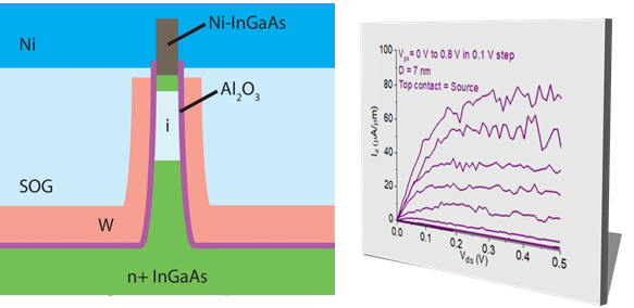
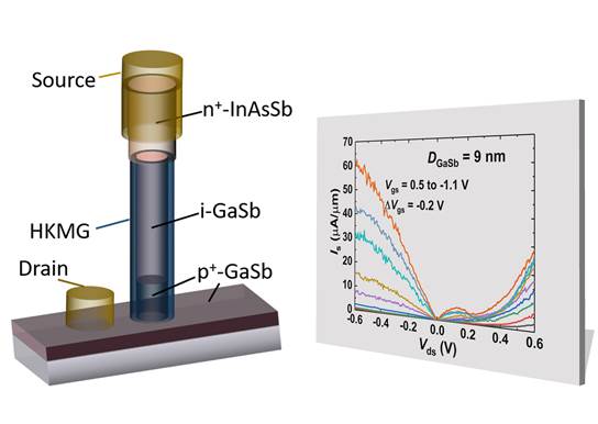
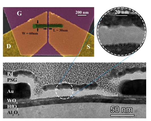
The Xtreme Transistors Group investigates novel nanoscale electronic device architectures based on new materials with the goal of expanding the frontiers of microelectronics to reach higher frequencies, higher speed, smaller size, extremely low power consumption, higher operating temperature, or to switch electrical power or amplify electrical signals at higher power levels. We have a particular interest on the potential of III-V and III-N compound semiconductors for new applications as well as novel devices for artificial intelligence applications.
Our research is eminently experimental. We design and fabricate our own prototype devices at the facilities of MIT.nano, the new nanoscale fabrication facility at MIT. We then characterize their operation in our own measurement laboratory. We also study the reliability of transistors and other devices under prolonged electrical, thermal and environmental stress. We build models and carry out simulations in order to understand the underlying physics. All our research is performed in close connection with industrial partners.

|

|

|

