Metal-Oxide Transistors and Ferroelectric Memory Devices for CMOS integration
Back-End of the Line (BEOL) technology has received great attention in the past few years, as front-end Si CMOS faces increasing scaling challenges beyond the 3 nm node. Metal oxides based on Si-compatible metals can be deposited with high quality at relatively low temperature and can form the basis for electronics that are embedded inside the interconnect structure of CMOS chips. Many field-effect transistor (FET) demonstrations based on a whole menu of metal oxides have been realized. In fact, FETs based on InGaZnO (IGZO), the most mature metal-oxide channel material, are widely used in active-matrix LCD and organic LED displays. IGZO-FETs are also under investigation for DRAM applications.
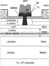
Our group is investigating the potential of In-based amorphous oxide semiconductors for BEOL electronics that are characterized by very low power consumption and very high density of integration. As such, we are focused on the development of enhancement-mode, or normally-off, transistors with nanometer-scale footprint. At the same time, adding the non-volatile memory (NVM) function to the BEOL platform is of great interest for emerging compute-in-memory (CiM) architectures dedicated to efficient implementation of artificial intelligence algorithms. In this application, dense memory demands highly-scaled devices in both the length and the width directions. Towards this, we are investigating BEOL ferroelectric (FE) FETs that integrate FE hafnium-zirconium-oxide (HZO) as gate material on an AOS-based transistor.
Recent publications:
RC-310 Shao, Y., E. R. Borujeny, J. Navarro, J. C.-C. Huang, T. E. Espedal, D. A. Antoniadis and J. A. del Alamo, Discrete Domain Switching in Scaled Oxide-Channel Ferroelectric FETs. 82nd IEEE Device Research Conference (DRC 2024), College Park, MD, June 23-26, 2024. (slides)

|


