Ultra-scaled Vertical Tunneling Transistors for Energy-efficient Electronics
In the last few years, we have witnessed an explosive progress in the ability of artificial intelligence and deep learning algorithms to tackle seemingly intractable problems of great human relevance. But these extraordinary accomplishments, based on very large models operating on enormous data sets, have also brought to the fore the urgency of dramatically enhancing the energy efficiency of computation. It is clear that future progress in AI will not be possible without a drastic reduction of the power consumption of microelectronics.
Lately, progress in Si complementary metal-oxide semiconductor (CMOS) technology, the main stream microelectronics hardware, has been slowing down, both in terms of supply voltage scaling and transistor footprint scaling. The former is limited by fundamental electron statistics that limit the sharpness of the turn-on characteristics of the metaloxidesemiconductor field-effect transistor (MOSFET). The latter is curtailed by severe short-channel effects when the transistor dimensions scale below tens of nanometers. In order to overcome the thermionic limit of the turn-on characteristics while maintaining a MOSFET-like drive current at a reduced operating voltage, tunnel field-effect transistors (TFETs) have attracted great interest for some time. However, experimental demonstrations to date have been disappointing. It is now commonly believed that there is a fundamental trade-off between high tunneling current and steep turn-on slope.
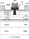
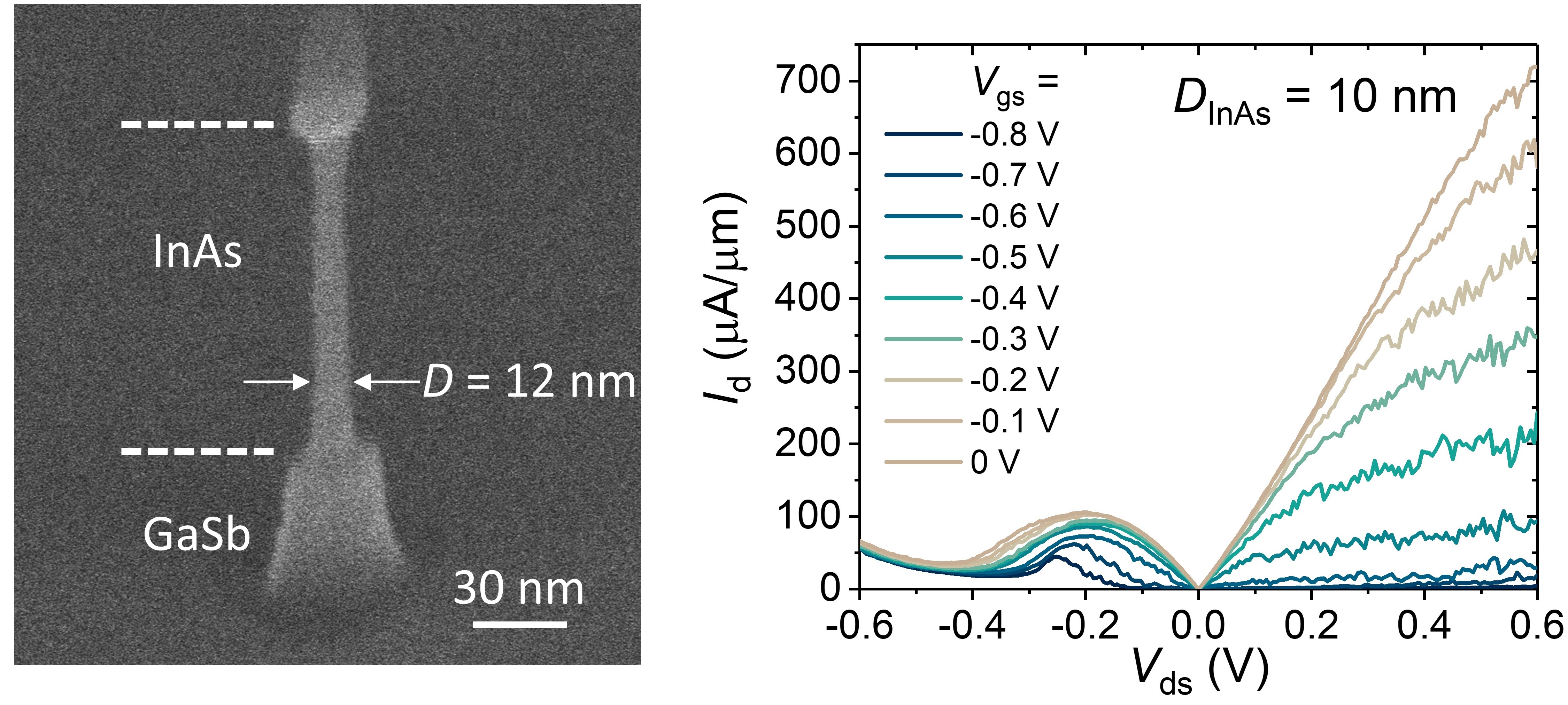
There are good reasons to believe that experimental demonstrations of TFETs to date have left much of the potential of this device architecture unexplored by overlooking the most promising regime of the design space, the strong quantum confinement regime at nanometer-scale dimensions. In our work, we explore this regime in the most promising material system for TFETs: the GaSb/InAs hetero-system with its favorable broken-band alignment for tunneling, and with the most scalable device architecture: the vertical nanowire (VNW) geometry. We experimentally demonstrate an unexpected but beneficial, significant HJ tunneling rate enhancement that yields TFETs with record electrical characteristics. This breakthrough discovery suggests that ultra-scaled HJ tunneling transistors can simultaneously meet the three stringent requirements for a future CMOS technology, i.e., steep current switching, high current drivability, and ultimate footprint scalability. These three attributes have never been demonstrated simultaneously in any emerging transistor concept.
Our work demonstrates a technology platform that can be highly scaled in terms of both supply voltage and footprint, which is extremely promising for future high-performance and ultra-low-power logic applications.
Recent publications:
RJ-227 Shao, Y., M. Pala, H. Tang, B. Wang, J. Li, D. Esseni and J. A. del Alamo, " Realizing the potential of ultra-scaled tunneling electronics through extreme quantum confinement. To be published in Nature Electronics.
RJ-218 Shao, Y. and J. A. del Alamo, "Sub-10 nm Diameter Vertical Nanowire p-Type GaSb/InAsSb Tunnel FETs. IEEE Electron Device Letters, Vol. 43, No. 6, pp. 846-849, June 2022. DOI
RJ-216 Shao, Y., M. Pala, D. Esseni and J. A. del Alamo, "Scaling of GaSb/InAs Vertical Nanowire Esaki Diodes Down to Sub-10 nm Diameter. IEEE Transactions on Electron Devices, Vol. 69, No. 4, pp. 2188-2196, April 2022. DOI
RJ-297 Shao, Y., M. G. Pala, D. Esseni, and J. A. del Alamo, Sub-10-nm Diameter GaSb/InAs Vertical Nanowire Esaki Diodes with Ideal Scaling Behavior: Experiments and Simulations. 2021 IEEE International Electron Devices Meeting (IEDM 2021), San Francisco, CA, December 11-15, 2021, pp. 677-680. DOI Sides
|