On April 29, 2014, MIT announced the launch of MIT.nano, a new facility that when finished will provide advanced capability for research and education across a wide range of nanoscale subjects.
Researchers at MIT are actively investigating both fundamental science and applications in many areas of nanotechnology. This activity takes place at MIT in individual laboratories and at joint centers and laboratories, such as the Microsystems Technology Laboratories (MTL). Given the scale of nanotechnology activity at MIT, the University has made a core decision to create a brand new research facility that will enable an increased pace of knowledge generation in this key area. The new building is called MIT.nano. The research activity to take place at MIT.nano will be highly interdisciplinary and will include work in fields such as energy, health, life sciences, quantum sciences, electronics, and manufacturing. In addition to providing unique capabilities for MIT researchers, the doors of MIT.nano will be open to academics from other universities and to scientists and engineers from national laboratories and companies, both large and small.
The benefits of having a core, interdisciplinary nanotechnology facility are numerous. The facility and the equipment it contains will be far more sophisticated and diverse than any individual research group can afford. A professional technical staff will both maintain the equipment and train users in its operation. Users across a range of disciplines will have the opportunity to work together on projects of mutual interest.
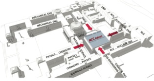
Preliminary construction work began in June 2014 and the building is scheduled for occupancy in 2018. It will be built on a central location at the site presently occupied by Building 12 and will be interconnected with major MIT buildings at multiple points, promoting easy access and frequent interactions.

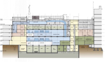
The new structure will be a 215,000-square-foot (21,000 m2) building, with class 100 and class 1000 clean room environments. Imaging spaces will be capable of reaching VC-G vibration criteria, which exceeds the mechanical quietness level needed for the use of even the most sensitive nano-scale instruments presently available. Prototyping spaces will allow a wide variety of devices to be fabricated. The combined fabrication and imaging space will be approximately 25,000 square-feet, double that available in the existing MTL facilities. An estimated 2,000 MIT and affiliated researchers may ultimately make use of the building in diverse areas of study.

MIT.nano has been designed to be the most sustainably built structure of its kind. From over 100 different sustainability options for integration into the building, 50 were selected for the final design. Building design innovations include heat recovery, variable air flow in chemical hoods and air filtering units, extensive environmental monitoring, and many other building structure innovations.
MIT.nano will also provide a unique teaching environment that will incorporate educational spaces on every one of its levels, revolutionizing the way we teach hands-on education. The basement level features a unique open classroom containing a wall of computer screens that allow the instructor to teach the class while projecting the results of experiments that are simultaneously happening in the neighboring nano-imaging labs. The lower and upper level clean rooms will be outfitted with video-camera feeds enabling real-time interaction between the users/instructors inside the clean environment and students/collaborators on campus or anywhere in the world. The direct video link will dramatically enhance our ability to teach and demonstrate the most advanced nano-scale processes, exposing participants outside the facility to the latest in-lab technology advancements. In addition, on the third level MIT.nano will house a computer-aided visualization environment (CAVE) room that will be interchangeably used either as a classroom or as a research lab. The CAVE is where theoretical and experimental ideas collide, enabling researchers to visualize matter on an atomic level in an immersive environment and to conduct virtual testing of theory, designs, and prototypes. Often compared to a "holodeck," this stunning facility will be a powerful teaching tool for nanoscience and nanotechnology.
The central location of MIT.nano will ensure that it serves as an innovation hub, enabling cross-pollination of disciplines. It will also be a convening place for academics and industrial collaborators. Our experience at MTL has demonstrated that the key for effective knowledge transfer between academia and industry is close interaction, co-location of investigators, and joint pursuit of research goals. Through these interactions our industry partners benefit both from research activity and access to outstanding students as potential employees.
A short video describing MIT.nano can found here
Other stories about MIT.nano:
--William Holber, Microsystems Technology Laboratories