MTL Day at Applied Materials
April 26, 2012

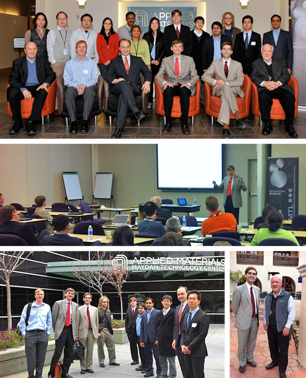
TOP: Group photo in lobby of Applied Materials. CENTER: Prof. Jesus del Alamo explains post-Si CMOS to the audience. BOTTOM, LEFT: Members of the MIT and Applied contingencies pose in front of the entrance to the Maydan Technology Center. BOTTOM, RIGHT: Prof. Tomas Palacios, left, with Dr. David Kyser of Applied Materials.
The MTL day at Applied Materials was organized by Dr. David Kyser of Applied Materials and MTL Associate Director Prof. Judy Hoyt. The day's schedule included:
- 9:15
- Prof. Vladimir Bulovic
MTL's Role in Advancing Efficient Lighting and Solar Technologies
- 10:00
- Prof. Tomas Palacios
GaN, Graphene, and other Extreme Materials for Future Electronics
- 10:45
- Break
- 11:00
- Dr. Om Nalamasu
Technology Challenges for Applied Materials
- 11:15
- Prof. Jesus del Alamo
Post-Si CMOS
- 12:00
- Lunch
- 1:00
- Prithu Sharma
High Efficiency Photovoltaics using III-V on Si Tandem Cells
- 1:20
- Jordon Chesin
III-V Nitride Nanowires for Light Emitting Diodes
- 1:40
- Dr. Kikang Kim
Synthesis of Graphene and Hexagonal Boron Nitride by Chemical Vapor Deposition
- 2:00
- Dr. Michael Swanwick
Large Array CNT Field Emitters with Integrated Gates
- 2:20
- Break
- 2:40
- Jae-Byum Chang
Block Copolymer Self-assembly for High Throughput Nanopatterning
- 3:00
- Matthias Bahlke
Dry Lithography of Large Area, Thin Film Organic Semiconductors Using Frozen CO2 Resists
- 3:20
- Apoorva Murarka
Novel Thin Film Processing for Large-area MEMS
- 3:40
- Photo
- 4:00
- End
